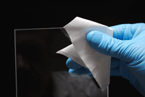
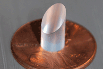
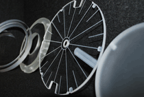
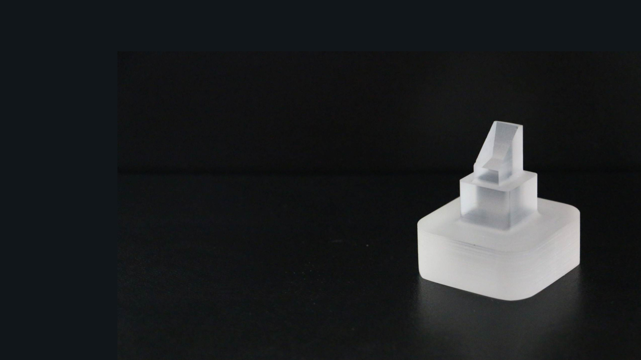
Mark Optics is manufacturing a prism for Harvard University’s Cohen Lab. Adam E. Cohen, PhD. and his team, develop some of the world’s … [Read More...] about Mark Optics provides Prism for Harvard’s Cohen Lab
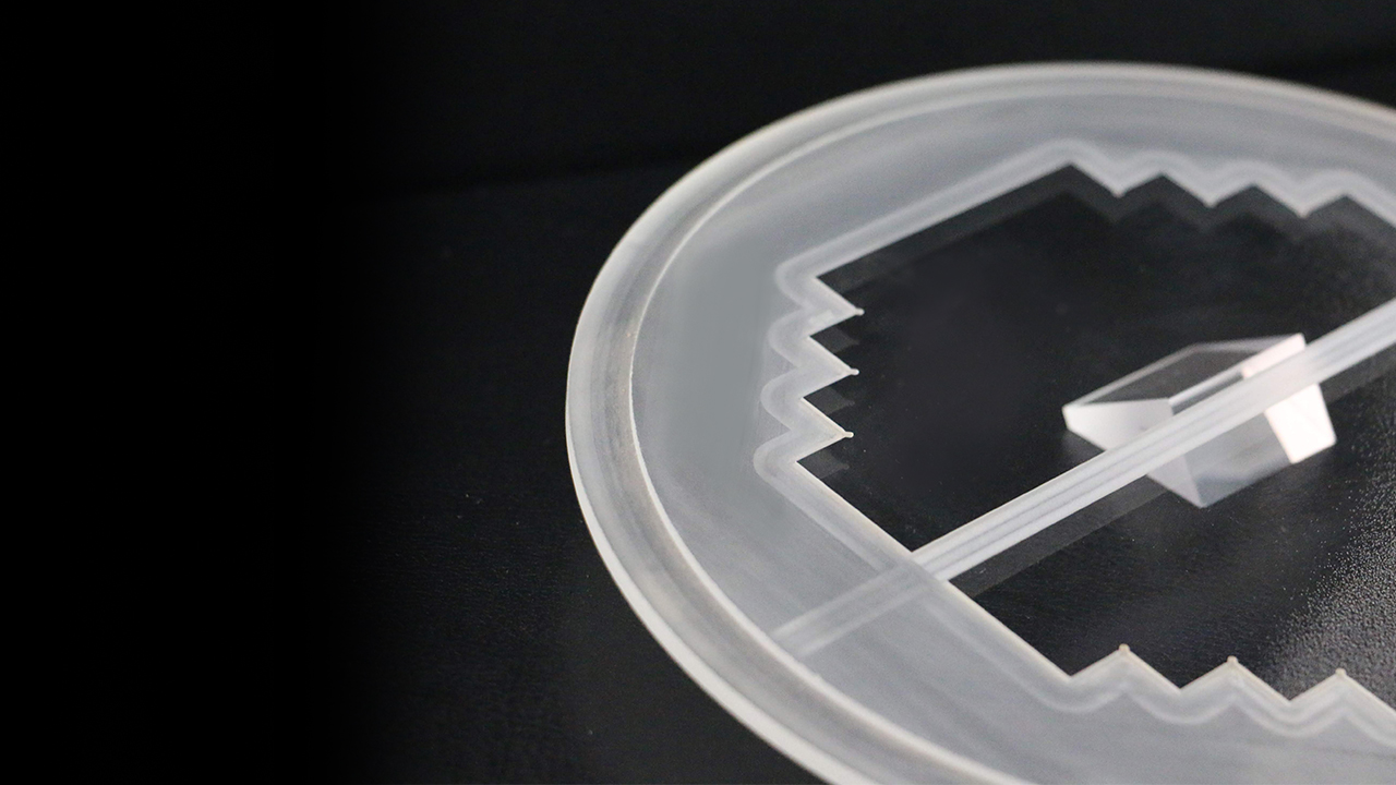
CNC Machining
Quartz
and Glassware
for Aerospace,
Semiconductor
and Optical Industries
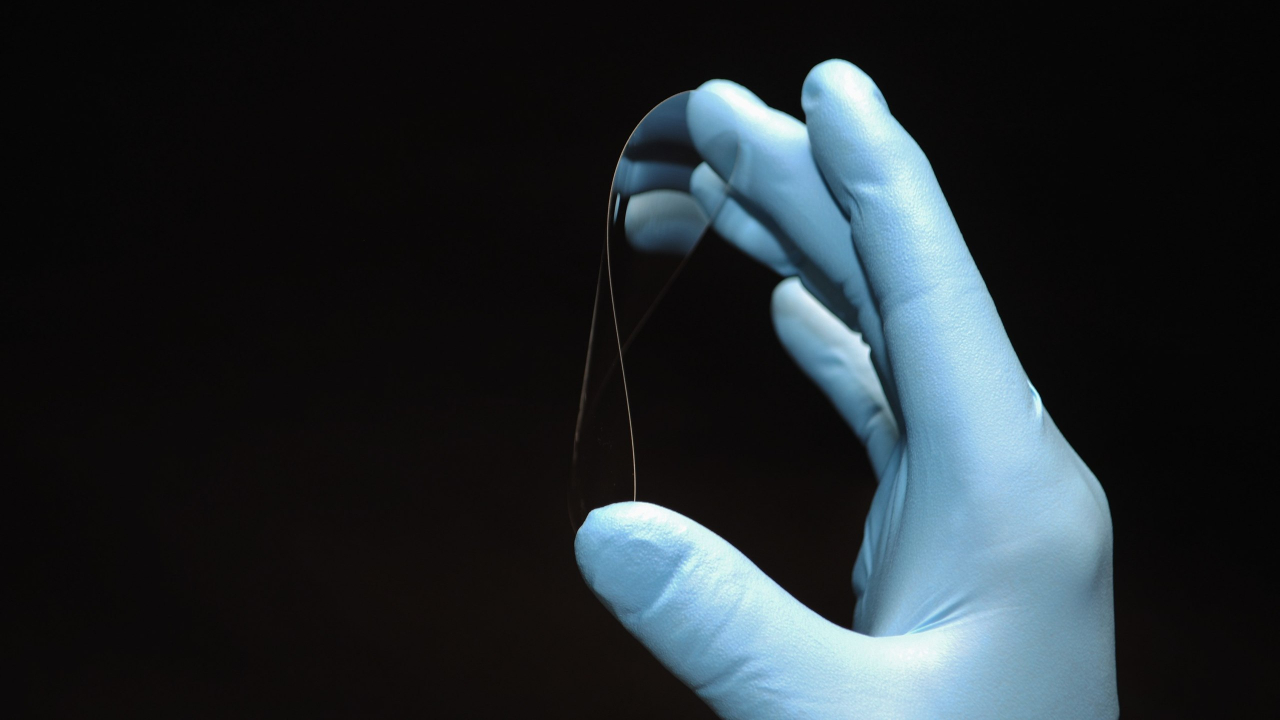
Need Thin?
25 μm Minimum Thickness

Founded in 1967 – Quality That Surpasses Generations.
ITAR Registered - ISO 9001 Compliant
ISO 9001-2015 Compliant
Custom Optics
We welcome your
creative ingenuity and ideas.
We believe it is people who solve problems.
We listen collectively, we collaborate scientifically,
we manufacture precisely.
Specialty Optical Components
only by Mark Optics
Mark Optics is a contract manufacturer of optical components specializing in extremely thin optical substrates and thinning/modifications of customer supplied substrates.
With over 30 different machine stations in our Santa Ana, California facility, we offer a wide collection of unique capabilities to our customers, all under one roof. We start with UV, Visible or IR raw materials and offer ID sawing, CNC shaping, edging, back thinning, etc. The shaping work centers support our finishing capabilities that range from OD polishing, precision flatness and surface roughness polishing as well as chamfering, ultrasonic cleaning, interferometer and CMM inspection to name a few. We work with parts as large as 20” square and as small as 2mm. Mark Optics is known in the industry as the company that is willing to make the extra effort to make a project successful. We are a small, agile, honest, ITAR Registered, ISO 9001-2008 compliant company that has been family owned since 1967. We welcome innovative manufacturing projects with challenging specs and lead times.
Products and Services
Thin Optical Substrates
Thinning Wafers (Substrates) Back Grinding or Back Thinning.
Mark Optics’ team of highly-skilled optical engineers – coupled with its unique processing capabilities – allows the company to continue pressing the physical limitations of thinning substrates.
We have successfully polished one inch diameter glass wafers to a
thickness of 25 µm, and are working on going even thinner. We have polished 100mm wafers to 50 µm thickness out of fused silica, Schott Borofloat 33, and other optical materials and crystals. Additionally, Mark Optics polishes shaped substrates, including: squares, hexagons and rectangles.
Optical Wafers
Manufacturing of company’s optical wafers include additional procedures that help minimize surface defects, fractures or micro-cracks that sometimes occur during fabrication. Typically, they have shown improved control during dry and wet etching, even during nanoscale processes. The wafers can be customized and made of any optical glass. As well, glass optical wafers can be custom made to meet a customer’s specific performance requirements.
Latest News
Mark Optics at SPIE Photonics West
Mark Optics, Inc. will be attending SPIE Photonics West in San Francisco this February. We look forward to seeing our clients and industry friends as … [Read More...] about Mark Optics at SPIE Photonics West
Mark Optics is ITAR Registered
Mark Optics is now ITAR registered. Due to the technical capabilities of Mark Optics' products and services, it was natural to have our company ITAR … [Read More...] about Mark Optics is ITAR Registered

