• Skip to main content
  • Skip to footer

Mark Optics Incorporated ~ Celebrating Over 5 Decades of Excellence ~ Founded in 1967

  • LinkedIn
  • YouTube
Mark Optics

Mark Optics

Mark Optics Incorporated ~ Celebrating More Than 53 Years Of Excellence ~ 1967-2018

714-545-6684     RFQ – Optical Substrate RFQ - Wafer
  • Home
  • About
  • Testimonials
  • Products
    • Product List
    • Recent Projects
    • Thin Optical Substrates
    • Wafer Substrates for Wafer Level Optics (WLO)
    • Product Photo Gallery
  • Capabilities
    • Standard Wafer Specifications
    • Maximum Precision Capabilities
    • Cleanroom Standards
    • Wafer Thinning
    • Ultra-Thin Fused Silica Wafers for Metasurface Innovation
  • Materials
    • Fused Quartz
    • Fused Silica
    • Low Expansion Material
    • Glass
  • Resources
    • Maximum Precision Capabilities
    • Standard Wafer Specifications
    • ISO 14644-1 Cleanroom Standards
    • Scratch / Dig Specifications
    • Standard Geometric Characteristics and Symbols
    • Refractive Index
  • Request a Quote
    • Request for Quote – Wafers
    • Request for Quote – Optical Substrate
  • Careers
  • Contact Us

Thin Optical Substrates

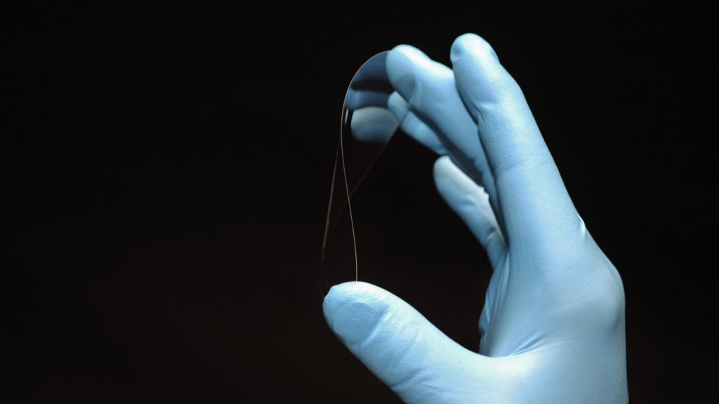
Mark Optics manufactures the thinnest optical substrates, wafers, and thin coverslips. Our unique processing capabilities allow us to continue to challenge the physical limitations of thinning wafers. We have successfully polished 1” glass wafers to thicknesses of 25 micron (0.001”) and are working on achieving 15 microns (0.0006”). When necessary, TTV and parallelism can be controlled to +/- 5 microns (0.0002”) or better. We have successfully polished 100mm round wafers to 50 micron thicknesses out of fused silica and Schott Borofloat 33 materials. We are able to polish different shaped substrates as well (squares, hexagons, rectangles etc.). We are here to work with your engineers on these challenging substrates.

Optical Substrates

Mark Optics has worked with numerous research organizations and universities to carefully identify the different requirements of different wafer usage. Using this feedback, Mark Optics has come up with three distinct processes for the fabrication of our wafers. Which one we will use will depend on the collaboration and information the customer provides. We are not a one size fits all organization. Instead, together we make a decision that will ensure wafers that works for you.

Complete our online RFQ form with your specifications.

ITAR Registered

Founded in 1967 – Quality That Surpasses Generations.
Request a Quote - Optical Substrate

Request a Quote - Wafer

Footer

Mark Optics Incorporated

Celebrating more than 53 years
of excellence from 1967.

– ITAR Registered – ISO 9001 Compliant
– ISO 9001-2015 Compliant

Green Policy

Mark Optics is committed to providing quality optical components through environmentally responsible business practices.

Made in the USA – A California Corporation

Mailing Address:
1424 East St. Gertrude Place
Santa Ana, CA 92705

Phone: (714) 545-6684

  • LinkedIn
  • YouTube

By continuing to browse the site, you are agreeing to our use of cookies.

Please see our privacy policy for more information.

Copyright © 2025 Mark Optics Inc. All rights reserved. Return to top