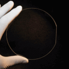
 Wafer Level Optic (WLO) fabricators have a need for super polished glass and fused silica/quartz wafers that have the same characteristics as conventional laser windows. Over the years, Mark Optics has worked with numerous research organizations and universities to carefully identify and control wafer surfaces and offer options to our customers.
Mark Optics wafers and substates are used in a multitude of WLO (Wafer Level Optics). As feature sizes get smaller it is even more important to ensure your UV, IR and visible materials are pure and the resulting wafers are optical quality before you start. Mark Optics wafer processes are specifically designed to fit your processing needs. Whether you are machining, etching, coating or bonding, we can customize our process to meet your requirements. We can also help you understand defects you may be finding from other wafer substrate suppliers. If you find you are seeing defects after machining or etching it is too late. Uniformity of quality is what you depend on and what we offer.
Our customers include many well-known wafer-level fabrication companies promising wafer level optical solutions for environmental sensing, 3D sensing, , AR, biometrics and microlens arrays to name a few. Whether you need just a few wafers to get started on your idea or large quantities of wafers for your production, Mark Optics can help.
Semi-Standard Quartz Wafers:
These are standard quartz (natural); fused silica (synthetic) wafers used primarily for semiconductor process verification and are sometimes referred to as “dummy” wafers. By specifying the surface roughness, this type of wafer is often used in plasma bonding or anodic bonding to silicon wafers (SOQ). . A double side polished wafer typically transmits greater than 90% between 260nm to 2.60 micron and has a refractive index of 1.4585. Surface roughness typically is Ra < 50 Angstrom
Semi-Standard Glass Wafers:
Our borosilicate wafers typically transmit visible through 2.40 micron when a CTE (coefficient of thermal expansion) similar to silicon is desired. These wafers can generally be used in thin film deposition, anodic bonding and as optical aligners to silicon wafers. Refractive indices range from 1.472 – 1.510 depending on material.
Optical Wafers:
These wafers have additional custom processes that have effectively minimized surface defects and sub-surface damage (“micro-cracks” and fractures) that can be introduced during fabrication. They typically have a surface roughness of Ra < 5 angstrom and have shown improved control during dry and wet etching even at nanoscale processing. Optical wafers can be custom made out of any optical glass that is required in your application. We collaborate with you to custom process your wafers to successfully perform in your clean room using your methods.
Fused silica optical wafers allow the maximum transmission from 180nm through 2.60 micron. This is optimal when your application is requiring the lowest light scattering characteristics while performing consistently during etching using standard or non standard MEMS processing.
Glass Optical Wafers can also be manufactured to specifically meet your requirements in performance.
Thin Wafers/Substrates:
Our unique processing capabilities allow us to continue to challenge the physical limitations of thinning wafers. We have successfully polished 1” glass wafers to thicknesses of 25 micron (0.001”) and are working on achieving 15 microns (0.0006”). When necessary, TTV and parallelism can be controlled to +/- 5 microns (0.0002”) or better. We have successfully polished 100mm round wafers to 50 micron thicknesses out of fused silica and Schott Borofloat 33 materials. We are able to polish different shaped substrates as well (squares, hexagons, rectangles etc.). We are here to work with your engineers on these challenging substrates.
