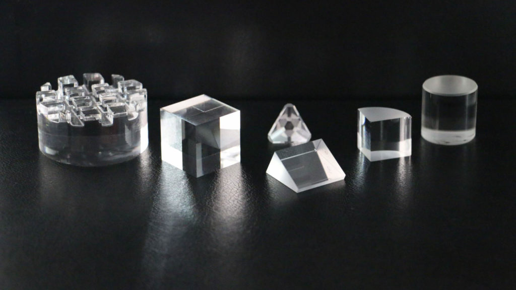
Mark Optics is a contract manufacturer of optical components specializing in extremely thin optical substrates and thinning/modifications of customer supplied substrates. With over 30 different machine stations in our Santa Ana, California facility, we offer a wide collection of unique capabilities to our customers, all under one roof. We start with UV, Visible or IR raw materials and offer ID sawing, CNC shaping, edging, back thinning, etc.
See our completed, ongoing, and signature optical manufacturing projects below.
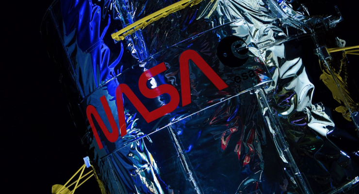


- Sustainable Land Imaging Technology, NASA Earth Science and Technology Office
- SPHEREx , Spectro-Photometer for the History of the Universe, Epoch of Reionization and Ices Explorer
- Cal Tech Palomar Observatory Zwicky Transient Facility (ZTF) Substrates for Telescopes
- Spider
- MAKO Detector
- Center for Clean Air Policy (CCAP), Chile
- Multicolor Submillimeter Inductance Camera (MUSIC) Telescope, Caltech Submillimeter Observatory (CSO)
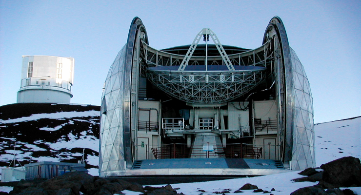
- Cal Tech Submillimeter Observatory (CSO), Mauna Kea, Hawai’i
- MUSTANG2 (Green Bank Telescope)
- SuperSpec, an On-Chip, MM-Wave, Filter-Bank Spectrometer
- BICEP2, South Pole Station, Antarctica
- Keck Array, South Pole Station, Antarctica
- Cosmic Microwave Background (CMB)
- POLAR
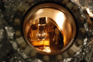
- Kinetic Inductor Detectors
- microPNT
- CYRA Infrared Spectrometer, Big Bear Solar Observatory (BBSO)
- ITER – https://www.iter.org/ International Thermonuclear Experimental Reactor